 |
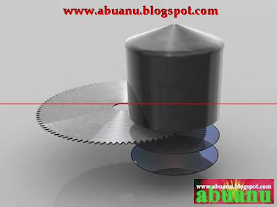
| A mono-crystal ingot is produced from electronic grade silicon. One ingot weighs approximately 100 kilograms (or 220 pounds) and has a silicon purity of 99.9999 percent. |
 |
| The photo resist layer protects wafer material that should not be etched away. Areas that were exposed will be etched away with chemicals. |
 |
| After the etching, the photo resist is removed and the desired shape becomes visible. |
 |
| After the ion implantation, the photo resist will be removed and the material that should have been doped (green) now has alien atoms implanted. |
 |
| The copper ions settle as a thin layer on the wafer surface. |
 |
| The excess material is polished off leaving a very thin layer of copper. |
 |
| After tests determine that the wafer has a good yield of functioning processor units, the wafer is cut into pieces (called dies). |
 |
| This is an individual die, which has been cut out in the previous step (slicing). The die shown here is a die of an Intel Core i7 processor. |
 |
| A microprocessor is the most complex manufactured product on earth. In fact, it takes hundreds of steps and only the most important ones have been visualized in this picture story. |
 |
| During this final test the processors will be tested for their key characteristics (among the tested characteristics are power dissipation and maximum frequency). |


No comments:
Post a Comment
வருகைக்கு நன்றி,
தங்களின் ஆலோசனைகளையும், கருத்துகளையும் சொல்லிவிட்டு செல்லுங்கள். மீண்டும் வருக.